- 您现在的位置:买卖IC网 > Sheet目录1992 > CY28551LFXC-3T (Silicon Laboratories Inc)IC CLOCK INTEL/AMD SIS VIA 56QFN
CY28551-3
....................Document #: 001-05677 Rev. *D Page 17 of 28
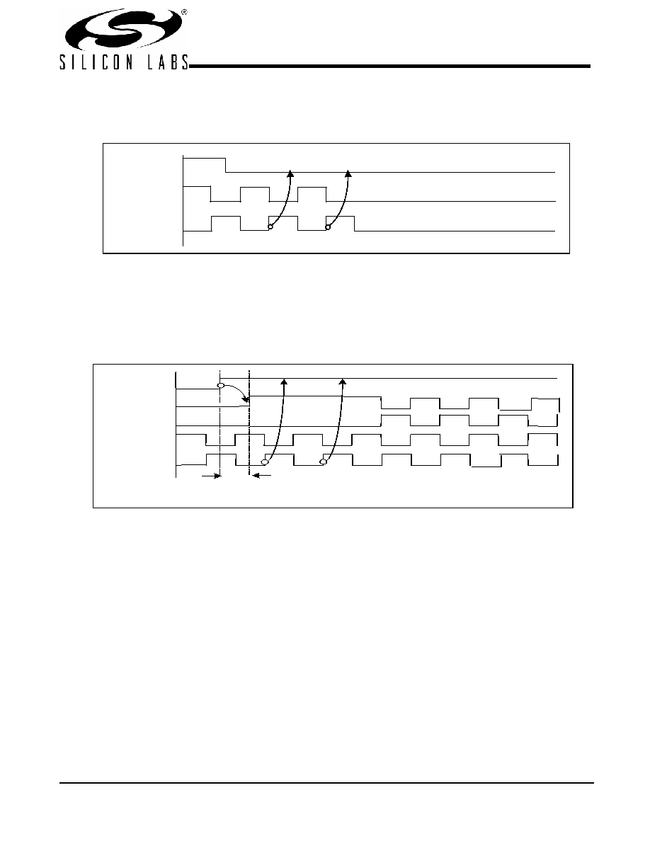
CPU_STP# Assertion
The CPU_STP# signal is an active low input used for
synchronous stopping and starting the CPU output clocks
while the rest of the clock generator continues to function.
When the CPU_STP# pin is asserted, all CPU outputs that are
set with the SMBus configuration to be stoppable via assertion
of CPU_STP# will be stopped after being sampled by 2-6
rising edges of the internal CPUC clock. The final state of the
stopped CPU clock is Low due to tristate, both CPUT and
CPUC outputs will not be driven.
CPU_STP# De-Assertion
The de-assertion of the CPU_STP# signal will cause all CPU
outputs that were stopped to resume normal operation in a
synchronous manner. Synchronous manner meaning that no
short or stretched clock pulses will be produce when the clock
resumes. The maximum latency from the de-assertion to
active outputs is between 2-6 CPU clock periods (2 clocks are
shown). If the control register tristate bit corresponding to the
output of interest is programmed to '1', then the stopped CPU
outputs will be driven high within 10ns of CPU_Stop#
de-assertion to a voltage greater than 200mV.
PCI_STP# Clarification
The PCI_STP# signal is an active low input used for cleanly
stopping and starting the PCI and PCIEX outputs while the rest
of the clock generator continues to function. The PCIF and
PCIEX clocks are special in that they can be programmed to
ignore PCI_STP# by setting the register bit corresponding to
the output of interest to free running. Outputs set to free
running will ignore both the PCI_STP# pin.
PCI_STP# Assertion
The impact of asserting the PCI_STP# signal will be the
following. The clock chip is to sample the PCI_STP# signal on
a rising edge of PCIF clock. After detecting the PCI_STP#
assertion low, all PCI and stoppable PCIF clocks will latch low
on their next high to low transition. After the PCI clocks are
latched low, the stoppable PCIEX clocks will latch to low due
to tristate as show below. The one PCI clock latency as shown
is critical to system functionality, any violation of this may result
in system failure. The Tsu_pci_stp# is the setup time required
CPU_STP#
CPUT
CPUC
Figure 5. CPU_STP# Assertion Timing waveform
C P U _ ST P#
CP UT
CP U C
CP UT In t e r n a l
T d r iv e _ C P U _S T P #, 10n S > 200 m V
CP U C In t e r n a l
Figure 6. CPU_STP# De-Assertion
发布紧急采购,3分钟左右您将得到回复。
相关PDF资料
CY28551LFXC
IC CLOCK INTEL/AMD SIS VIA 64QFN
CY2SSTV855ZXI
IC CLOCK DIFFDRV PLL DDR 28TSSOP
CY2SSTV857ZXI-27
IC CLK DDR266/333BUF1:10 48TSSOP
CY2SSTV857ZXI-32
IC CLK DDR266/333BUF1:10 48TSSOP
CY505YC64DT
IC CLK CK505 BROADWATER 64TSSOP
CYW150OXC
IC CLOCK 440BX AGP 56SSOP
CYW173SXC
IC CLK GEN TAPE DRV 4CH 16SOIC
CYW305OXC
IC CLOCK W305 SOLANO 56SSOP
相关代理商/技术参数
CY28551LFXCT
功能描述:时钟发生器及支持产品 Universal System Clk Intel AMD SiS Via RoHS:否 制造商:Silicon Labs 类型:Clock Generators 最大输入频率:14.318 MHz 最大输出频率:166 MHz 输出端数量:16 占空比 - 最大:55 % 工作电源电压:3.3 V 工作电源电流:1 mA 最大工作温度:+ 85 C 安装风格:SMD/SMT 封装 / 箱体:QFN-56
CY2862-000
制造商:TE Connectivity 功能描述:82A0111-4-9-G110
CY2863-000
制造商:TE Connectivity 功能描述:82A0111-8-9-G110 - Bulk
CY28800
制造商:CYPRESS 制造商全称:Cypress Semiconductor 功能描述:100-MHz Differential Buffer for PCI Express and SATA
CY28800OXC
功能描述:时钟缓冲器 PCI Express & Sata Diff Buffer 100MHz RoHS:否 制造商:Texas Instruments 输出端数量:5 最大输入频率:40 MHz 传播延迟(最大值): 电源电压-最大:3.45 V 电源电压-最小:2.375 V 最大功率耗散: 最大工作温度:+ 85 C 最小工作温度:- 40 C 封装 / 箱体:LLP-24 封装:Reel
CY28800OXCT
功能描述:时钟缓冲器 PCI Express & Sata Diff Buffer 100MHz RoHS:否 制造商:Texas Instruments 输出端数量:5 最大输入频率:40 MHz 传播延迟(最大值): 电源电压-最大:3.45 V 电源电压-最小:2.375 V 最大功率耗散: 最大工作温度:+ 85 C 最小工作温度:- 40 C 封装 / 箱体:LLP-24 封装:Reel
CY28800OXI
功能描述:时钟缓冲器 PCI Express & Sata Diff Buffer 100MHz RoHS:否 制造商:Texas Instruments 输出端数量:5 最大输入频率:40 MHz 传播延迟(最大值): 电源电压-最大:3.45 V 电源电压-最小:2.375 V 最大功率耗散: 最大工作温度:+ 85 C 最小工作温度:- 40 C 封装 / 箱体:LLP-24 封装:Reel
CY28800OXIT
功能描述:时钟缓冲器 PCI Express & Sata Diff Buffer 100MHz RoHS:否 制造商:Texas Instruments 输出端数量:5 最大输入频率:40 MHz 传播延迟(最大值): 电源电压-最大:3.45 V 电源电压-最小:2.375 V 最大功率耗散: 最大工作温度:+ 85 C 最小工作温度:- 40 C 封装 / 箱体:LLP-24 封装:Reel